Technology
NT&D is a leader in Nanoimprint technology with over 15 year of experience.
Furthermore, we provide you with the whole process technology for fabrication of wide range of devices including:
|
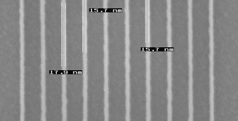
15nm lines imprinted in UV curable resist |
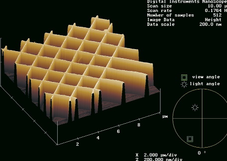
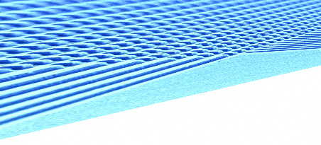
Simultaneous Pattern replication of micro- and nano features.
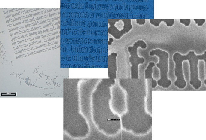
Analogue Imprint: Pattern replication and transfer into silicon of the first page of the Gutenberg's Bible (B. Vratzov, A. Fuchs, INFO PHYS TECH 34, 2001)
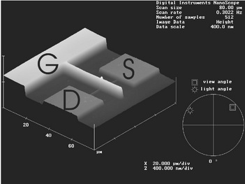
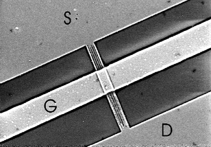
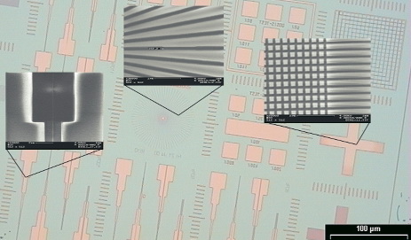
Single channel NMOSFET, 100nm channel width (left), multi-channel NMOSFET, 50nm channel width (right)
Through our collaboration with MESA+, one of the largest nanotechnology research institutes, we have access to the NanoLab that includes following facilities:
1250 m2 fully equipped cleanroom with focus on:
800 m2 laboratory space:
|
 |